


Developed in the mid-1980s in several university and industrial labs, QWIP technology arose from the confluence of bandgap engineering afforded by compound-semiconductor heterostructures, and ultra-high-vacuum epitaxy techniques such as molecular beam epitaxy (MBE) and metalorganic chemical vapor deposition (MOCVD).
Unlike photovoltaic (PV) or photoconductive (PC) detectors that rely on interband (valence band to conduction band) absorption in semiconductors, QWIPs rely on intersubband absorption of light between quantized energy states in quantum wells within the conduction/valence band.
Such square quantum wells usually consist of GaAs layers sandwiched between AlGaAs barriers: the GaAs layer thickness determines the well width, the Al% in the barrier AlGaAs controls the well depth. By adjusting these two parameters, quantum wells can be created having two bound states with an energy separation that can be controlled to be anywhere from ~ 3 µm to ~ 20 µm. The wells are doped to provide electrons in the ground state which resides near the well bottom. Incoming photons with the right energy pop/excite these electrons to the excited state that is designed to be near the well top, from where they are swept out by an applied voltage. QWIPs thus have a sharp spectral response, dictated by the sharpness of the quantized states. A QWIP is the simplest and most striking manifestation of quantum mechanics - the classic "particle-in-a-box" problem in any QM textbook.
The cost and performance advantages of QWIP technology arise from the maturity of GaAs/AlGaAs growth and process technology. For example, QmagiQ FPAs are fabricated on wafers upto 6-inches in diameter and use the latest and best growth and process tools. This automated production guarantees the best sensitivity, uniformity, and reproducibility.

Why indeed. In a nutshell, cost and performance. If you want a high-performance large (320x256 and larger) 2D LWIR FPA in this lifetime at reasonable cost, QWIP technology is the only way to go. Sure, MCT technology is only two years away, and has been for the last 20 years. But if you want results, not promises, and have products to deliver with limited budgets, you cannot afford to not look at QWIPs. It will save you time and money, and deliver performance. Guaranteed.
The physics, technology, and advantages of QWIPs are captured in the following snapshot charts.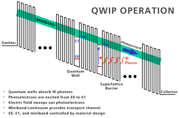
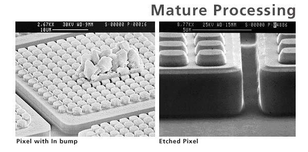
- Vertical sidewalls (RIE)
- Precise control of small patterns (RIE)
- Narrow trenches between pixels
- High fill-factor (> 87% in 320x256 FPA)
- High-yield wafer-level process
- 3-inch and 6-inch automated wafer handling
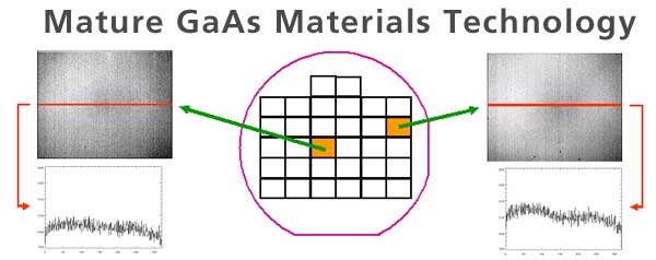
- Mature MBE/MOCVD growth process
- Multi-wafer growth reactors (upto 15 3-inch wafers per growth run)
- Quality control procedures in place
- High uniformity
- Superior wafer-to-wafer reproducibility
- Excellent lot-to-lot reproducibility
- Material cost is low and continues to drop as volume increases
- Maximum GaAs wafer size = 6-inches
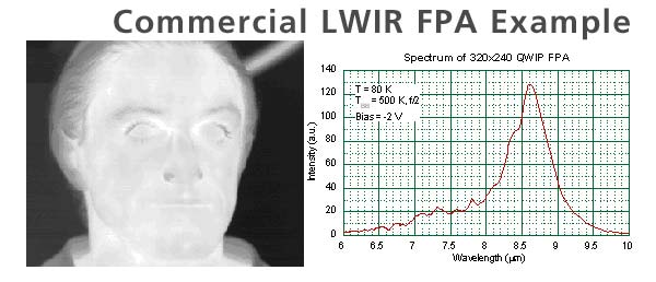
- 320x256x1 format (XxYxSpectral-band)
- Pitch = 30 µm
- LWIR (peak wavelength at ~ 8.6 µm)
- Fill-factor > 87%
- Operability >> 99.5%
- Non-uniformity < 3% uncorrected
- NETD < 20 mK (@ 60K, f/2, 100 Hz)
- QE = 15%, CE = 5%
- Operating Temperature = 65 - 77K
- In production
- Pixels isolated electrically & optically
- 3 bumps per pixel
- Vertical sidewalls
- Small vias
- > 80% fill-factor top color
- > 85% fill-factor bottom color
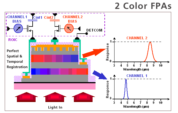
- Architecture Advantages
Ł Narrow QWIP spectral response ideal for multi-color applications
Ł No optical filter required
Ł No signal-processing required
Ł Spatially-registered images
Ł Simultaneous integration
Ł Wide range of spectral band combinations possible
Ł Single-chip solution dramatically lowers size, power, and cost of multi-band imaging
- Peak wavelength as low as 4.0 µm achievable in QWIP
- Shorter wavelength detection achieved with integrated pin diode
