


QWIPs promise to reduce the cost of IR imaging
Vision Systems Design September, 2004
Author : Andrew Wilson
For years, the US government has spent millions of dollars perfecting IR devices based around mercury cadmium telluride (HgCdTe). Fragile and expensive, this material is difficult to grow defect-free, which reduces wafer yields and results in the high manufacturing costs of large IR focal-plane arrays. As an alternative, quantum-well infrared photodetectors (QWIPs) are now being offered by a number of companies. Offering better uniformity, these detectors are challenging HgCdTe detectors in the IR spectrum.
“The advantages of gallium arsenide (GaAs) QWIP technology over other IR detector technologies is the relative ease of fabrication, which translates to low production costs and high yield, the ability to spectrally tune the IR response of the detector over a broad portion of the IR region (3-18 µm), high pixel-to-pixel uniformity, and reduced low frequency (1/ƒ) noise,” says Murzy Jhabvala, chief engineer at the NASA Goddard Space Flight Center Instrument Technology Center (Greenbelt, MD, USA; www.gsfc.nasa.gov). At the center, scientists have developed a 1-Mpixel QWIP with a spectral response between 8.4 and 9.0 µm.
Like most commercially available QWIPs, the sensor operates by the photoexcitation of electrons between sub-bands of quantum wells fabricated by placing very thin layers of two different, high-bandgap semiconductor materials alternately on a GaAs base or template. “By adjusting the thickness of the GaAs layer and the concentration of aluminum in the AlGaAs barriers, it is possible to control both the thickness and height of the quantum well,” says Mani Sundaram, president of QmagiQ (Nashua, NH, USA; www.qmagiq.com), a commercial designer and manufacturer of QWIPs. “By controlling the quantum-well width and the barrier height, inter-sub-band transition energy can be varied to enable IR detection at any wavelength range between 3 and 20 µm"
The development of QWIPs, however, could not have emerged without a confluence of technologies. To control the quantum-well width and the barrier height, uniformly pure semiconductor layers must be grown on large substrate wafers to a fraction of a molecular layer. “This task has only recently been possible through the use of modern crystal-growth methods such as molecular-beam epitaxy and metal-organic-chemical -vapor-deposition systems,” says Sundaram.
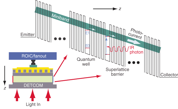
In the design of QWIP devices, absorption of IR photons excites electrons from the ground state of a quantum well to an excited state close to or within an adjacent energy-transport band. This causes a photocurrent that can be detected and further processed.
To generate an imager based on QWIP tchnology is also not simple. Unlike CCDs, on which charge collected at each photosite can be shifted off-chip by embedded shift registers, it is difficult and expensive to fabricate on-chip shift registers using materials such as GaAs. Because of this, signals from each individual detector element must be read out individually using a second semiconductor device known as a readout integrated circuit (ROIC). To manufacture the hybrid sensor, the QWIP must be flip-chip bonded to the ROIC in a process that involves fabricating indium bumps onto contact holes, one per pixel, on both the detector chip and the ROIC. These two devices are then aligned and mated by applying heat and mechanical force.
Two patents currently cover the manufacture of these devices. The first, obtained by Martin Marietta Labs, now part of Lockheed Martin (Baltimore, MD, USA; www.lockheedmartin.com), was transferred to BAE Systems (Nashua, NH, USA; www.na.baesystems.com). After licensing this technology in 2003, QmagiQ has produced a number of IR detector arrays including the Falcon256 (a 320 × 256 array), the Falcon240 (a 320 × 240 array), and the Hawk512 (a 640 × 512 element array). The Falcon256 is beginning to be used in two commercial IR cameras on the market.
According to Axel Reisinger, chief technical officer at QmagiQ, the noise equivalent temperature difference (NETD)-the smallest target temperature difference that can be detected with the devices-is better than 20 mK at ƒ/4. “Compared with typical uncooled microbolometer devices with an NETD of 100 mK at ƒ/1, this is an enormous improvement,” he says.
In 1994, the second QWIP patent, initially obtained by Bell Laboratories (Murray Hill, NJ, USA; www.bell-labs.com), was transferred to The Jet Propulsion Laboratory (JPL; Pasadena, CA; www.jpl.nasa.gov). Since then, it has been licensed by QWIP Technologies (Altadena, CA, USA; www.qwip.com), which also offers three devices based on the technology. The largest, the QWIPCHIP 1024 × 1024 long-wavelength IR focal-plane array, features a spectral band center of 8.6 µm ±0.1 µm, a pixel size of 18 µm, and an 85% fill factor.
According to QmagiQ’s Sundaram, the difference between the two patented approaches relates to how barriers in the QWIP are constructed, which affects the electron transport band (specifically how the states in this band are distributed in energy). This transport band, which energetically resides above the conduction band of the quantum well, determines the manner of transport of electrons with specific energy generated by the interaction of IR radiation with electrons in the quantum well. >From a fundamental physics viewpoint, the two methods are very similar, except that the resulting QWIP is sensitive to different material design parameters.
Vision Systems Design September, 2004
Author : Andrew Wilson
